
PCB Cloning: Understanding the Process and Its Applications
2025-03-04
In the world of electronics, the importance of printed circuit boards (PCBs) cannot be overstated. These integral components serve as the foundation for almost all electronic devices, from smartphones to medical equipment. As technology advances, the demand for PCBs continues to grow, which has led to the emergence of a practice known as PCB cloning. In this blog, we will explore what PCB cloning is, how it works, and the applications and benefits it offers in the field of electronics.
What is PCB Cloning?
PCB cloning is the process of duplicating an existing PCB design, typically for the purpose of replication or reverse engineering. This process involves extracting the layout, components, and design specifications of a PCB and reproducing it as a new, functional board. In essence, it is a way to create an identical or similar copy of an existing circuit board without access to the original design files.
The cloning process can be performed in several steps, including image capture, circuit analysis, and the recreation of the board design. This can be done for a wide range of reasons, from creating replacement parts for outdated or discontinued devices to learning and experimenting with existing designs for innovation and improvement.
The PCB Cloning Process
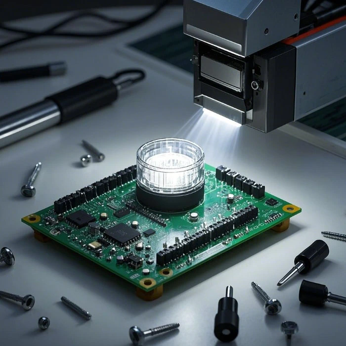
1. Physical Examination of the PCB
The first step in PCB cloning involves examining the original board. This typically includes taking high-resolution photographs or scans of both sides of the PCB. These images serve as a reference for replicating the layout and identifying the components used on the board. Detailed analysis of the traces, pads, vias, and other features of the PCB is essential for creating an accurate clone.
2. Schematic Diagram Creation
The next step involves converting the physical PCB layout into a schematic diagram. This step is critical because it allows engineers to understand the function of the PCB and how the components are interconnected. Creating the schematic may involve manually tracing the connections between components, which can be a time-consuming but necessary task for ensuring an accurate clone.
3. Component Identification and Selection
After the schematic diagram is created, the next step is to identify the components used on the original board. This includes understanding the types of resistors, capacitors, transistors, integrated circuits (ICs), and other electronic components used. Once identified, engineers select the appropriate components to use in the cloned PCB, ensuring that they meet the required specifications for functionality and compatibility.
4. Designing the PCB Layout
With the schematic diagram and component list in hand, the next step is to design the PCB layout. This involves placing the components on the board and routing the electrical traces that connect them. Specialized PCB design software is often used to create the layout, ensuring that the traces are properly routed and the board meets manufacturing requirements.
5. Prototyping and Testing
Once the PCB layout is complete, the next step is to create a prototype of the cloned PCB. This prototype is assembled using the selected components, and the board is thoroughly tested to ensure it functions correctly and meets the desired specifications. Any issues identified during testing can be addressed before the final version of the PCB is produced.
6. Mass Production (if necessary)
If the cloned PCB is intended for large-scale production, the design is sent to a PCB manufacturer who will produce the board in bulk. The manufacturer uses the design files to create the boards, and after assembly, the cloned PCBs are tested again to ensure their quality and performance.
Why Clone a PCB?
There are several reasons why PCB cloning might be necessary or beneficial:
1. Replacement for Discontinued Products
One of the most common reasons for PCB cloning is to replace outdated or discontinued products. In many industries, older devices or machinery may rely on specific PCBs that are no longer in production. Cloning the PCB allows companies to continue using these devices without having to redesign the entire system or purchase expensive replacement parts from third-party sources.
2. Reverse Engineering for Innovation
PCB cloning is often used in reverse engineering, where engineers analyze an existing design to learn from it and create improved versions of the original product. This process allows for innovation in the field of electronics, as engineers can take inspiration from existing designs and modify them to meet new needs or incorporate new technologies.
3. Cost Reduction
Cloning a PCB can be a cost-effective alternative to designing a new circuit board from scratch. By duplicating an existing design, companies can save on research and development costs, as well as reduce the time required to bring a new product to market. Cloning also allows for the reuse of components and layouts that have already been proven to work effectively.
4. Educational Purposes
PCB cloning is often used for educational purposes, especially in electronics and engineering programs. By replicating existing designs, students and hobbyists can learn about the inner workings of electronic devices and gain hands-on experience with PCB design and manufacturing. It also offers a valuable opportunity to practice reverse engineering and circuit analysis.
5. Repairs and Maintenance
PCB cloning can be essential for repairs and maintenance, especially when dealing with older equipment. If a specific PCB has malfunctioned and no original replacements are available, cloning the PCB allows technicians to create a working replacement and extend the life of the equipment.
Applications of PCB Cloning
PCB cloning is used in various industries and applications, including:
1. Consumer Electronics
Many consumer electronics devices, such as smartphones, laptops, and gaming consoles, use complex PCBs. PCB cloning is often used to repair damaged or outdated circuit boards, as well as to create compatible replacement parts for discontinued products.
2. Automotive Industry
The automotive industry relies on a wide range of electronic systems, from infotainment to engine control units. PCB cloning is used to produce replacement parts for electronic systems in vehicles, especially for older models where the original parts are no longer available.
3. Medical Devices
In the medical field, PCB cloning is often used to replace critical components in devices like diagnostic equipment, pacemakers, and monitoring systems. Ensuring the availability of replacement parts through PCB cloning is crucial for maintaining the operation of these life-saving devices.
4. Industrial Equipment
Many industrial machines rely on custom PCBs for control and monitoring functions. PCB cloning helps ensure that these machines remain operational by providing replacements for damaged or obsolete circuit boards.
Conclusion
PCB cloning is a valuable process that plays a significant role in the world of electronics. Whether it is for replacing discontinued parts, reverse engineering for innovation, or ensuring the longevity of existing equipment, PCB cloning offers a practical solution to a variety of challenges. As technology continues to evolve, the ability to clone PCBs will remain an essential tool for engineers, manufacturers, and hobbyists alike. By understanding and leveraging PCB cloning, we can ensure that electronics remain functional, cost-effective, and innovative for years to come.