

OEM Aixtron G5+ GaN Epitaxy Susceptor Key Considerations for GaN Manufacturers
2026-11-16
Every GaN manufacturer running an Aixtron G5+ knows the susceptor isn’t just another consumable—it’s the stage where uniformity, yield, and uptime are decided. But what should you actually evaluate before choosing an OEM or aftermarket replacement? Thermal cycling stability, coating integrity, and dimensional tolerance can make or break a production run. Semicorex tackles these variables head-on, so you can focus on the epi, not the hardware. Here’s a closer look at the factors that really matter.
Why Susceptor Material Choice Sets the Ceiling for GaN Wafer Uniformity
The susceptor is never a passive tray in GaN epitaxy. It sits directly between the heating source and the wafer, so its thermal conductivity, emissivity, and heat capacity define the temperature distribution that reaches the growing film. Even a perfectly tuned reactor cannot correct for a susceptor that releases heat unevenly or has local variations in coating thickness. Those subtle differences in temperature across the wafer surface become locked into the GaN layer as thickness gradients, doping drift, or changes in indium incorporation, and no amount of gas flow tuning can fully erase them.
Material stability under process conditions is equally decisive. Graphite, SiC-coated graphite, and refractory metals all respond differently to prolonged exposure to ammonia and hydrogen at high temperature. A coating that slowly roughens or reacts with the process gas changes its emissivity over time, which shifts the thermal profile run after run. At the same time, outgassing or micro-particle release from the susceptor can disturb nucleation and coalescence locally, producing regions of higher dislocation density or different surface morphology. These effects accumulate and set a practical ceiling on wafer uniformity that no process recipe can overcome once the susceptor material itself becomes the dominant source of variation.
The choice of susceptor material also controls the thermal response during ramp-up and cool-down, not just at steady state. High thermal mass materials smooth out short-term fluctuations but can also create lag that leaves the wafer edge cooler than the center for critical portions of the growth. Conversely, low thermal mass materials may follow the heater too quickly and amplify small heater imbalances. Either way, the room for improvement is bounded by the intrinsic uniformity of the material properties and coating quality. That is why the susceptor is often the true limiter: it sets the highest achievable level of GaN wafer uniformity before other process variables even come into play.
Thermal Expansion Mismatch and the Early Failure of G5+ Susceptors
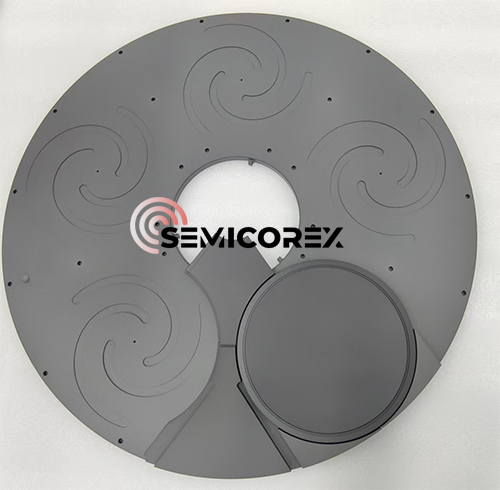
In high-temperature epitaxial processes, G5+ susceptors are subjected to rapid thermal cycling that exposes the inherent mismatch between silicon carbide coatings and graphite substrates. The coating expands at a slightly lower rate than the underlying graphite, generating interfacial shear stresses that accumulate with each heating and cooling cycle. These stresses concentrate at geometric discontinuities such as pocket edges, wafer pockets, and gas flow channels, where microcracks initiate well before the expected service life. Unlike gradual wear, this early failure mode often manifests as sudden coating delamination or particulate generation, compromising both wafer yield and chamber cleanliness.
The severity of thermal expansion mismatch is amplified by the non-uniform temperature distribution across large-diameter G5+ susceptors. During ramp-up, central regions heat faster than the periphery, creating transient thermal gradients that drive differential expansion within the same plane. Combined with the through-thickness mismatch, this leads to a complex stress state that cannot be fully relieved by creep in the graphite core. Repeated cycles then propagate microcracks along the coating-substrate interface, eventually causing localized spallation. Field data from production fabs indicate that susceptors exhibiting such early failures often show a characteristic pattern of crack networks aligned with high-stress zones, rather than uniform wear.
Mitigating this issue requires rethinking both material pairing and susceptor geometry. Coatings with tailored coefficient of thermal expansion values closer to graphite, or functionally graded interlayers that dissipate stress, have shown promise in extending service intervals. Additionally, redesigning pocket transitions with larger radii and avoiding sharp steps reduces stress concentration factors. Some manufacturers are exploring alternative substrate materials with lower anisotropy, while others implement slower ramp protocols to minimize transient gradients. Until these solutions become standard, G5+ susceptors remain vulnerable to premature failure driven by thermal expansion mismatch, impacting throughput and maintenance costs in advanced semiconductor fabs.
Coating Shedding and Particle Control in High-Volume GaN Production
Maintaining clean surfaces in high-volume GaN production often comes down to how well the deposition chamber resists micro-delamination. Early in a tool's life, coating shedding can go unnoticed because the flakes are too small to trigger immediate yield loss. Over time, though, thermal cycling and repeated wafer loads create stress concentrations at the interface between the chamber coating and the underlying metal. Once those stresses exceed a critical threshold, the coating begins to spall in tiny fragments that drift onto process wafers or backside handling surfaces. Rather than waiting for particle counts to climb, production teams track chamber history and replace coatings well before visible wear appears.
Particle control in GaN epitaxy depends heavily on gas flow uniformity and the physical design of the susceptor. Any sharp edge, bolt hole, or unpolished zone acts as a nucleation point for gas-phase reactions that leave particulates behind. Standard practice involves using refractory materials with matched thermal expansion coefficients, so that repeated ramp-up and cool-down cycles do not create micro-cracks. Process engineers also adjust carrier gas dynamics so that particulate-laden flows are directed toward exhaust rather than across the wafer plane. This is not a one-time fix; it requires continuous monitoring of both particle maps and wafer backside haze after every run.
A less obvious but equally important factor is the way coating materials age under alternating process chemistries. GaN tools frequently switch between ammonia-rich and hydrogen-rich conditions, which can strip surface oxides unevenly. That uneven stripping weakens the coating bond and accelerates shedding. Teams that run long production campaigns mitigate this by inserting short stabilization steps between recipe changes and by periodically conditioning the chamber with a sacrificial coat. The payoff shows up in lower particle-related scrap and fewer unplanned tool opens, both of which matter more as wafer volumes climb into the thousands per month.
Specifying Susceptor Flatness When Wafers Bow More Than Expected
When wafer bow exceeds the range assumed during susceptor design, a simple global flatness callout rarely holds up. The actual contact area between wafer and susceptor shifts under process temperature, so specifying a single TTV or bow number can miss local gaps that disrupt heat transfer. It is more practical to map the wafer's deformed shape across several production lots and use that profile as the reference surface.
A better approach is to define flatness in terms of the matching error between the susceptor and the bowed wafer, rather than an absolute plane. For convex wafers, a slight concave pocket in the susceptor center can restore contact; for concave wafers, the opposite may be needed. Some fabs specify a zonal flatness budget—tighter in the center, relaxed near the edge—or ask for a custom-ground profile based on measured bow data.
Verification should also move away from room-temperature metrology. Thermal expansion of both parts changes the gap, so a hot chuck test or a simulated process soak is the only way to confirm the specification works. Sharing the wafer bow distribution and temperature recipe with the susceptor vendor allows them to grind or lap a compensating surface, and the final acceptance criterion becomes the temperature uniformity on the wafer backside rather than a standalone flatness number.
The Real Cost Gap Between OEM and Aftermarket Susceptors
Most buyers start by comparing invoice prices, but the real cost gap between OEM and aftermarket susceptors rarely shows up on a purchase order. An OEM unit might cost 30-40% more up front, yet it often carries tighter tolerance controls for film thickness and metal deposition. That consistency can mean fewer rejected product runs and less downtime, which matters more on high-speed packaging lines than in a single test kitchen.
Aftermarket susceptors, on the other hand, are not automatically the cheaper option once you factor in replacement frequency and energy draw. Some lower-priced films heat unevenly or degrade faster under repeated microwave cycling, forcing you to raise power settings or swap rolls mid-shift. But there are also aftermarket suppliers that have closed the quality gap without the OEM markup—especially for standard, low-temperature applications where exotic substrates are not required.
The cost gap, then, becomes less about brand and more about matching the susceptor's thermal profile to your actual load. Running a small pilot batch with an aftermarket sample alongside your current OEM stock usually reveals more than any spec sheet. If the defect rate stays flat and the roll change interval holds, the savings are real; if not, the OEM premium is paying for itself in avoided scrap.
Cleaning Cycles That Preserve Coating Integrity on Aixtron G5+ Parts
On Aixtron G5+ reactors, the cleaning cycle must be tuned to the specific coating chemistry rather than using a one-size-fits-all acid strip. Residual gallium, indium, or aluminum precursors bind differently to oxide and nitride barrier layers, so a stepped protocol works better: first a warm deionized water soak to loosen water-soluble byproducts, then a low-concentration organic acid bath at 40–45°C for no more than 20 minutes, followed by a pH-buffered neutralizer. This keeps the coating's grain structure intact instead of roughening it through repeated acid attack.
Abrasive media should stay out of the line entirely. Even soft brushes can leave micro-scratches that become nucleation sites for coating delamination under thermal cycling. For stubborn deposits on showerheads or wafer carriers, a low-energy plasma ash with oxygen or hydrogen can remove carbonaceous films while leaving the underlying ceramic or metallic coating unchanged. After every third wet clean, a short vacuum bake at 120°C drives out moisture from pores and helps close any micro-cracks before the part returns to process conditions.
Record bath conductivity and pH drift after each run to detect when the solution load is too high. If conductivity rises more than 15% from baseline, the bath is already saturating and will redeposit dissolved metals onto the coating, which later shows up as dark spots or early flaking. Filtering the post-clean rinse water and checking for particle counts above 0.3 µm gives an early warning before coating failure becomes visible.
FAQ
The susceptor controls how heat reaches each wafer pocket and how process gases flow across the surface. On the G5+ platform, even small deviations in pocket depth or coating thickness can shift the thermal profile enough to create variations in GaN thickness and doping. Keeping the original design geometry intact is what prevents center-to-edge non-uniformity from showing up in production.
An OEM susceptor is matched to the reactor's heating zones and gas flow patterns. Generic options often use slightly different graphite grades or coating methods, which can cause hot spots near the wafer edges or delayed thermal response. Those differences may not be obvious during a single run, but they accumulate as wavelength drift and sheet resistance spread across a lot.
Most G5+ susceptors use a silicon carbide coating over high-purity graphite. The SiC layer needs to be dense enough to resist ammonia and hydrogen at typical GaN growth temperatures. Before loading wafers, it is worth checking for pinholes, coating delamination, or uneven gloss. Any exposed graphite accelerates particle generation and metal contamination.
Watch for dull grey patches, edge chipping, or a rough surface texture after cleaning. These are signs the SiC layer is thinning or cracking. Also monitor wafer temperature readings: a slow drift in pyrometer values at the same heater power often means the susceptor's emissivity has changed locally.
Avoid aggressive in-situ etches unless they are truly needed, because chlorine-based cleaning wears the SiC coating faster than standard ammonia/hydrogen cycles. Limit rapid temperature swings at the start and end of each run, and use the recommended pocket fill pattern to keep thermal stress evenly distributed.
The G5+ handles larger wafer batches, so pocket depth directly affects heat transfer from the susceptor to each wafer. If pockets are too shallow, wafers can overheat; if too deep, they may not couple thermally with the pocket floor. Either condition increases bow, slip lines, and run-to-run variation in GaN thickness.
Inspect the wafer pockets under bright light for any color shift from black to grey, since that indicates a coating breach. Run a dry leak-back test on the reactor if possible. Store the susceptor in a nitrogen-purged cabinet and avoid touching the coated surfaces with bare hands, because oils from skin can create local nucleation defects.
Conclusion
For GaN epitaxy on Aixtron G5+ reactors, the susceptor is not a commodity part—it dictates how far wafer uniformity can actually go. The base material sets the ceiling: graphite grades with inconsistent thermal conductivity or poor resistance to thermal cycling will show up as thickness and doping drift across a run, no matter how well the recipe is tuned. One of the most common failure modes we see is early cracking or warping driven by thermal expansion mismatch between the graphite core and the SiC or ceramic coating. That mismatch does not just shorten service life; it creates micro-cracks that become particle sources. In high-volume production, coating shedding is the quiet killer. Once the protective layer starts to flake, particles land on the wafer surface and yield drops before anything shows up in routine metrology. So material selection and coating adhesion are not separate issues—they determine whether the chamber stays clean enough for repeatable GaN growth.
Flatness specifications also need a rethink when wafers bow more than the datasheet assumes. A susceptor that measures perfectly flat at room temperature can still cause poor thermal contact under process conditions because the wafer and pocket deform differently. GaN manufacturers often chase pocket depth and edge profile instead of just overall flatness. Then there is the cost question. OEM Aixtron G5+ susceptors carry a premium, but aftermarket parts vary wildly in graphite purity, coating thickness, and dimensional control. The real cost gap is not the purchase price—it is the lost runs from a susceptor that fails early or sheds particles. Finally, cleaning cycles matter more than most teams admit. Aggressive acid or plasma cleaning can erode the SiC coating, especially around pocket edges. A cleaning protocol that preserves coating integrity will extend the usable life of both OEM and qualified aftermarket susceptors, and that is where the actual savings show up.
Contact Us
Contact Person: Svenja Wei
Email: [email protected]
Tel/WhatsApp: +8613567891907
Website: https://www.semicorex.com